Wish me luck for the Presentation Day
INTELLIGENT HIGHWAY LAMP POST
Wednesday, December 18, 2013
Week 14 (FYP2) : Poster
Hi, this week is the week of the presentation day. So i had designed my poster, and showed it to my project advisor. She did correct my poster in term of the design and wording.
Sunday, December 8, 2013
Week 13 (FYP2) : Result and Analysis
Hi, this is the last week before the Presentation week. So i need to collect some data for my project.
I had measured the output voltage of the solar panel from 8am until 6pm.
I had measured the output voltage of the solar panel from 8am until 6pm.
The figure above shown the voltage reading of the solar panel, at 11am.
Time
|
8am
|
9am
|
10am
|
11am
|
12pm
|
1pm
|
2pm
|
3pm
|
4pm
|
5pm
|
6pm
|
Volt
|
9.57
|
10.23
|
11.8
|
13.02
|
13.9
|
13.5
|
13.2
|
12.43
|
11.29
|
10.18
|
9.02
|
Table above shown the data i managed to collect.
Besides measuring the output voltage of the solar panel, i also did measure the power consumption of the LED bulb.
The load (LED bulb) was rated at 12.26V and 0.11A.
Saturday, November 30, 2013
Week 12 (FYP2) : Troubleshooting
Hi, this week, i will be discuss about troubleshooting. Troubleshooting is a very important step, before you can present your project to your assessors. this is to prevent further humiliating, if the project not working.
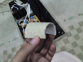
For my project, i had found 1 problem, and it was related to PIR sensors. Upon investigation, the problem was because of the range of detection for the both PIR sensor. It was known that PIR sensor has long and wide detection range, so range of detection for both PIR sensors, overlapped with each other. To solve this problem, I used a cardboard, and cover the PIR sensors. This is to limit their range of detection.
For my project, i had found 1 problem, and it was related to PIR sensors. Upon investigation, the problem was because of the range of detection for the both PIR sensor. It was known that PIR sensor has long and wide detection range, so range of detection for both PIR sensors, overlapped with each other. To solve this problem, I used a cardboard, and cover the PIR sensors. This is to limit their range of detection.
Figure above shown the range of detection for PIR sensor.
I had used cardboard, to cover the PIR sensors, and limit their range of detection
Wednesday, November 20, 2013
Week 10 & 11 (FYP2) : Assembling the solar panel with the structure
Hi, this week, i will combine the post for Week 9 and 10 together, since it took quite time to get done the structure. In case you don't know what structure i am talking about, please check it out here.
Solar panel was assembled on the structure of
the highway lamp post, and the connection was soldered.
Friday, November 8, 2013
Week 9 (FYP2) : Designing the structure
Hi guys. This week i had played around with SketchUp software, to design the structure of my highway lamp post. SketchUp is a freeware software, and very user-friendly. Even a noob like me, can use it :)
You can download it from here.
Thursday, October 31, 2013
Week 8 (FYP2) : Soldering the components
Hi, this week, i have soldered all components on the PCB. My skill a little bit rusty, because the last time i solder was when i was in Semester 3, for subject Electronics 2.
Since the PCB has been designed according to the
schematics diagram, so minimal wire jumper was needed.
This is the look of the PCB after the components has been soldered on it.
Saturday, October 26, 2013
Week 6 & 7 (FYP2) : Creating the PCB
Hi, sorry for late posting of the Week 6, because i was busy preparing for the Phase Test. So, i combined Week 6 and Week 7 under one post.
This week, i had create the PCB using layouts that i had designed using Altium Designer; and copper board. There were many step involved in creating the PCB.
This week, i had create the PCB using layouts that i had designed using Altium Designer; and copper board. There were many step involved in creating the PCB.
Figure above shown the process of cutting the copper board. i bought an A4 sized copper board in Jalan Pasar for RM9.
Figure above shown the cutting process of the OHP sheet.After printing the PCB layout on a Overhead Projector (OHP) sheet, i cut it according to the size.
Align the OHP sheet which has the printed layout
on the copper board. Make sure the
printed side was facing the copper side of the board.
Iron the OHP sheet onto the copper board. The
heat applied by the iron, will cause the ink on the OHP sheet to stick on the
copper board. Thus making the copper board look like the OHP sheet.
Dip the PCB into the Etching solution (Ferric
Chloride solution, FeCl3. The solution reacted with the unmasked
copper, and removes the unwanted copper from the PCB. This process is called as
Etching. The PCB was check every 10 minutes.
Now the PCB was carefully drilled, to make the
holes, using drilling machine.
Picture above is the completed PCB.
Subscribe to:
Comments (Atom)


